Sub-micrometer scanning probe based characterization of RF products on wafer-level (SuRF)
Project goals
- Development of a scanning probe based metrology system for sub-micrometer characterization and testing of RF semiconductor products
- Precision probe alignment and automation for in-device RF metrology
- Evaluation of millimeter-wave circuit characterization on device and wafer-level
Description
RF systems belong to the key components of modern technologies such as radar for environmental detection for safe automated driving through night and fog and Internet of Things devices like 5G telecommunication chips. State of the art RF probing systems have a limited spatial resolution due to large contact pads of conventional ground-signal-ground probes and cannot measure signals within the active area of the RF structures.
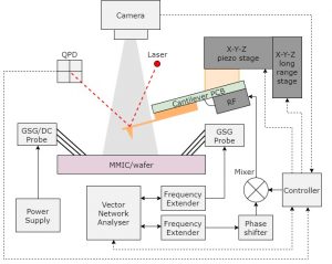
Concept of RF sensing scanning probe microscopy prototype for nanoscale structures and circuits
SµRF will address this shortcoming by developing a flexible and versatile RF microscopy system up to 90 GHz using conductive atomic force microscopy (AFM) cantilever, which facilitates precision down to nanometer scale. Advanced control and positioning algorithms with camera-based and optical AFM readout enable RF probing with automated probe alignment and nanoscale spatial resolution. The developed RF scanning probe system is verified on mmWave circuit devices (MMIC) and on wafer-level to validate the capability for production in-line metrology. The unique RF measurements enable design cycles to be reduced, chip size to be shrunk and improve RF and mmWave products to be designed with increased spatial precision.
Use case
- In-line metrology for production of radio frequency (RF) and millimeter wave (mmWave)
semiconductor system-on-a-chip circuits like radar and 5G telecommunication
Project partner
- Infineon Technology Austria AG
Funding
- Production of Future, FFG – Austrian Research Promotion Agency
- Infineon Technology Austria AG
Contact
Univ.-Prof. Dipl.-Ing. Dr.sc.techn. Georg SchitterDipl.-Ing. Mathias Poik
Project Staff
Dipl.-Ing. Mathias PoikDipl.-Ing. BSc. Thomas Hackl
Dipl.-Ing. Dr.-Ing. Richard Schroedter
Martin Schober