Sub-Mikrometer Rastersonden-basierte Charakterisierung von HF-Halbleiterprodukten auf Waferebene (SuRF)
Ziele
- Entwicklung eines rastersondenbasierten Metrologiesystems zur Submikrometer-Charakterisierung und Prüfung von RF-Halbleiterprodukten
- Präzise Tastkopfausrichtung und Automatisierung für die In-Device-HF-Messtechnik
- Bewertung der Charakterisierung von Millimeterwellen-Schaltungen auf auf Bauelement- und Wafer-Ebene
Beschreibung
HF-Systeme gehören zu den Schlüsselkomponenten moderner Technologien wie beispielsweise Radar für Umgebungserfassung zum sicheren automatisierten Fahren durch Nacht und Nebel und Internet der Dinge wie 5G-Telekommunikations-Chips. Nach dem Stand der Technik haben HF-Tastsysteme aufgrund der großen Kontaktflächen herkömmlicher Masse-Signal-Masse-Tastköpfe eine begrenzte räumliche Auflösung und können keine Signale innerhalb des aktiven Bereichs der HF-Strukturen messen.
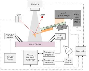
Konzept des flexiblen und versatilen HF-Mikroskopiesystems für die Charakterisierung nanoskaliger HF- und Millimeterwellenschaltungen
SuRF wird dies durch die Entwicklung eines flexiblen und versatilen HF-Mikroskopie-systems bis 90 GHz mit einer Positionsauflösung im Submikrometer-bereich unter Verwendung von leitfähigen Rasterkraftmikroskopie (AFM)-Cantilevern angehen. Fortschrittliche Steuerungs- und Positionierungsalgorithmen mit kamerabasierter und optischer AFM-Auslesung ermöglichen HF-Messungen mit automatischer Sondenausrichtung und räumlicher Auflösung im Nanometer-bereich. Das entwickelte HF-Scanning-Tastsystem wird an mmWave-Schaltkreisen und auf Wafer-Ebene verifiziert, um die Fähigkeit zur Inline-Metrologie in der Produktion zu validieren. Die einzigartigen HF-Messungen ermöglichen eine Reduktion der Designzyklen, die Verkleinerung der Chipgröße und den Entwurf innovativer HF-Produkte durch die erhöhte räumliche Präzision.
Anwendungen
- Inline-Messtechnik für die Produktion von Hochfrequenz- (RF) und Millimeterwellen- (mmWave) System-on-a-Chip Halbleiter-Schaltungen wie Radar und 5G-Telekommunikation
Projektpartner
- Infineon Technology Austria AG
Förderung
- Produktion der Zukunft, FFG – Austrian Research Promotion Agency
- Infineon Technology Austria AG
Ansprechpartner
Univ.-Prof. Dipl.-Ing. Dr.sc.techn. Georg SchitterDipl.-Ing. Mathias Poik
ProjektmitarbeiterInnen
Dipl.-Ing. Mathias PoikDipl.-Ing. BSc. Thomas Hackl
Dipl.-Ing. Dr.-Ing. Richard Schroedter
Martin Schober